Since electrospinning has been shown to allow controlled nanofiber deposition, there is an interest in its use to print conductive wire on circuit board. This would simplify the production of circuit board and increase the density of electronic components that can be packed on a circuit board. To realise this application, a few requirements must met. First the resultant nanowire must be of sufficient conductivity. Secondly, the precision, consistency and accuracy of nanowire deposition must be good enough. Thirdly, the performance of the nanowire must be adequate, consistent and reliable.
There are several ways to produce conductive nanowires from electrospinning. A conductive material that is electrospinnable is the most direct way of producing conductive nanowires. However, most conductive materials are not directly electrospinnable. Even for polyaniline, a conductive polymer, direct electrospinning requires modification of the setup such as using a coagulation bath [Razak et al 2015]. Cardenas et al (2007) used a acetone as the coagulation bath for the collection of electrospun polyaniline. The collected fibers were isolated on the collection bath instead of as a non-woven membrane which reflects the difficulty of fiber formation using neat polyaniline. The spread of its conductivity was also large ranging from 10-3 to 102 S cm-1. Fibers with larger diameter showed a higher conductivity than smaller diameter fibers. Given the difficulty in electrospinning conductive material directly, an alternative is to use electrospun conductive composite fibers.
In composite conductive electrospun fibers, there are several ways in which the conductive materials may be incorporated with the electrospun fibers. One of the most commonly used and simplest methods is through blending. However, in blended system, the conductive materials may be separated by non-conductive material that forms the matrix. A more effective method may be to coat the fibers with a conductive material or forming core-shell fibers. Between core-shell fibers and blended fibers, the conductive materials are constrained and more localized in a core-shell fiber and therefore have a higher conductivity. Comparing the conductivity of the MWCNT/polymer core-shell fibers from Wang et al (2014) and the blended MWCNT/polymer fibers from Wang et al (2012), the former was able to achieve a conductivity of 1 x 10⁻⁵ S/cm at 1.4 wt% MWCNT loading while the latter has a conductivity of just 1.86-8 S/cm with 10% loading. This showed that concentrating the MWCNT for better contacts more critical for better conduction than loading factor. In coated fibers, the surface coated conductive material will be in touch with one another which facilitate electron transport through the fibers. Kang et al (2007) simply coated electrospun silk membrane with MWCNT by dipping the membrane into a MWCNT suspension. The uniform coating and presence of numerous junctions for electron conduction gives the membrane a conductivity of 2 x 10⁻⁴ S/cm which is even higher than the core-shell MWCNT fibers from Wang et al (2014). Generally, metal is still a much better conductive material compared to polymer and polymer composites. While direct electrospinning of metal is not possible, there are a few indirect method of producing metallic nanowire through electrospinning.
A variety of methods are available for coating a conductive metallic layer on electrospun nanofibers. Metallic coatings such as chromium, gold, copper, silver and aluminum can be applied to electrospun nanofibers using thermal evaporation [Wu et al 2013]. Platinum and nickel has been coated on electrospun nanofibers using electron-beam evaporation and silicon and ITO using a.c. magnetosputtering [Wu et al 2013]. The coated nanofiber sheet can be transferred to a silicon substrate using dropcast. With a coating thickness of 100 nm on one side, the nanotrough layer is sufficiently strong to be self-supporting after the nanofiber templates have been removed [Wu et al 2013]. A single gold nanotrough was found to have an electric conductivity of 2.2 x 10⁵ S/cm which is slightly less than its polycrystalline bulk [Wu et al 2013].
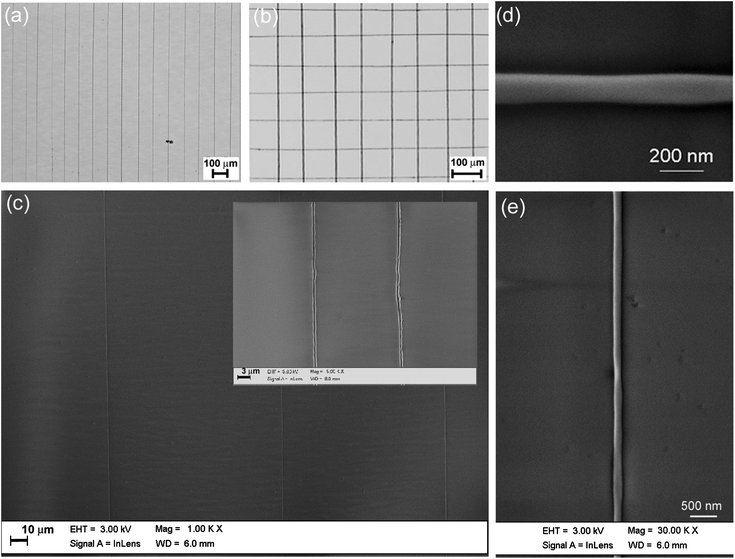
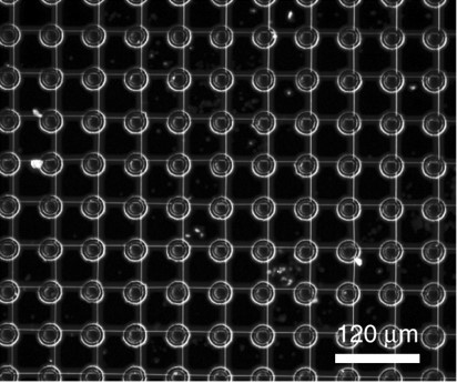
Other than sufficient material conductivity, the next challenge is to precisely and accurately deposit the nanofibers on a surface. Advances in directed electrospinning especially in near field electrospinning has seen great progress in the ability to deposit electrospun fibers precisely and accurately. In a demonstration of printed circuit board using electrospinning, Min et al (2013) used near field electrospinning to deposit semiconducting poly(3-hexylthiophene) (P3HT):PEO-blend organic nanowire over multiple field-effect transistors on a flexible polyarylate substrate at a speed of 13.3 cm/s with regular spacing of 50 µm and fiber diameter of 289 nm. They have also demonstrated the ability to spin highly aligned nanowires from other materials such as poly(9-vinyl carbazole) (PVK) and poly{[N,N'-bis(2-octyldodecyl)-naphthalene-1,4,5,8-bis(dicarboximide)-2,6-diyl]-alt-5,5'-(2,2'-bithiophene)}.
While many conductive polymers are difficult to electrospin directly into fiber without a carrier polymer, carbonization of electrospun polymer fibers to form carbon nanofibers offer an alternative path to construct electrospinning-based printed circuit boards. George et al (2020) showed that it is possible to use near field low voltage electrospinning deposit polyacrylonitrile (PAN) fiber with high precision especially when used with patterned carbon pillars on silicon substrate. These carbon pillars of diameter about 20 µm and spacing of less than 40 µm apart has been shown to be very effective in guiding the fiber to deposit on it even if the electrospinning jet was slightly offset by a small angle. However, when pillars are used to support the fibers, it is important to control the voltage. At relatively high voltage, the fiber diameter produced by near field low voltage electrospinning is thicker and this causes the wires to fall into the trenches due to slower solvent evaporation which weakens the fiber. During carbonization, the PAN fibers would shrink and this may result in breakages. The studies by George et al (2020) showed an 87% survival rate of suspended wires on 7 µm deep channels having a width <40µm. The resultant carbon fibers on the pillars have a diameter smaller than 40 nm.
For electrospinning to be used commercially as a method for electronic circuit board nanowire printing, precision and accurate nanowire deposition with a consistent wire conductivity value needs to be demonstrated. Currently, large industrial level nanofiber production is only used for random nanofiber membrane production. Investigation of near-field electrospinning using multi-nozzles is just at the nascent stage. Using electrospinning for prototyping of miniature circuit board may be a possible application with just a single nozzle.
Published date: 12 December 2017
Last updated: 06 June 2020
▼ Reference
-
George D, Garcia A, Pham Q, Perez M R, Deng J, Nguyen M T, Zhou T, Martinez-Chapa S O, Won Y, Liu C, Lo R C. Fabrication of patterned graphitized carbon wires using low voltage near-field electrospinning, pyrolysis, electrodeposition, and chemical vapor deposition. Microsyst Nanoeng 2020; 6: 7.
Open Access
-
Kang M, Jin H J. Electrically conducting electrospun silk membranes fabricated by adsorption of carbon nanotubes. Colloid Polym Sci 2007; 285: 1163.
-
Min S Y, Kim T S, Kim B J, Cho H C, Noh Y Y, Yang H C, Cho J H, Lee T W. Large-scale organic nanowire lithography and electronics. Nature Communications 2013; 4: 1773.
-
Razak S I, Wahab I F, Fadil F, Dahli F N, Khudzari A Z, Adeli H. A Review of Electrospun Conductive Polyaniline Based Nanofiber Composites and Blends: Processing Features, Applications, and Future Directions. Advances in Materials Science and Engineering 2015; 2015: 356286.
Open Access
-
Wu H, Kong D, Ruan Z, Hsu P C, Wang S, Yu Z. A transparent electrode based on a metal nanotrough network. Nature Nanotechnology 2013; 8: 421.
▲ Close list